


R5年度(2023)高柳研究奨励賞受賞
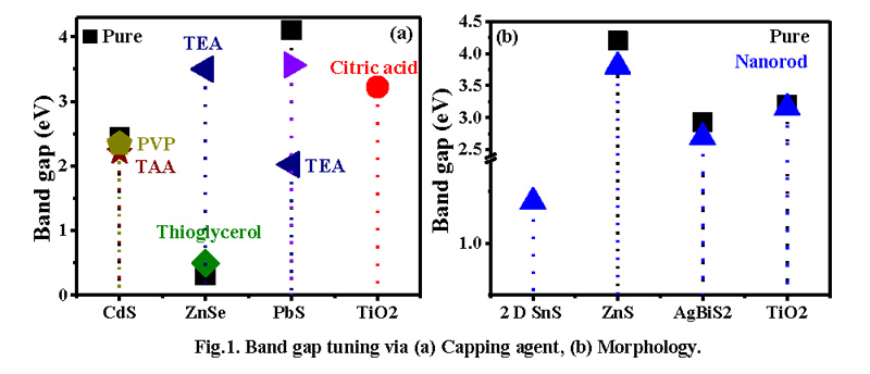
I have extensive research experience on tuning the optoelectronic properties of various nanomaterials (TiO2, PbS,CdS, ZnSe, CuInS2, MnS, ZnS, and ZnSe) for vivid electronic applications. The optoelectronic properties of the material depend upon several parameters including optical bandgap, surface morphology, intrinsic band structure of the material and so on. I have carefully tuned each of these parameters separately using diverse strategies and have achieved outstanding results in the above attempts. For instance, I successfully synthesized Al-doped TiO2 embedded graphene oxide using a hydrothermal method and identified that the introduction of metal doping into the TiO2 matrix significantly improved its optical properties by mitigating defects. This enhancement in the charge transport of the Al doped TiO2-GO nanocomposite was demonstrated in a study published in Applied Surface science, 449 (2018) 332-339). Similarly, I carried out the demonstration of CdS nanoflowers with a capped PVP, synthesized by precisely controlling the reaction time and temperature. The phase transition was observed from cubic to hexagonal leading to modified band structure of the material. This resulted in enhanced optical properties of CdS nanoflowers, identified via UV-vis absorption spectroscopy (Materials Research Bulletin, 94 (2017) 190-198). Apart from the usual nanostructures, I have also explored the synthesis of CuInS2/MnS/ZnS core-multishell nanocrystals using a hot injection method that led to increased stability at 543 and 752 nm. The significant utility of nanocrystals as an efficient bioimaging probe was highlighted by optical and structural characterization techniques (Ind. Eng. Chem. Res, 57(2018) 15703-15721). Correspondingly, the research was conducted on PbS nanocubes synthesized through a wet chemical method. By carefully controlling the reaction time and temperature, I managed to achieve monodispersed nanocubes with dimensions ranging from 10-15 nm. The size of these nanocubes was deliberately chosen to be smaller than the excitonic Bohr radius of bulk PbS, leading to effective utilization of quantum confinement effects. This research yielded promising results that can be actively inculcated in future applications of optoelectronic industries.(Materials Letters, 71 (2012) 44-47). I conducted several research on tuning the morphology of nanomaterial by several approaches to enhance its optical properties. For instance, I explored the one-step chemical synthesis of surfactant-free CdS nanospheres and tailored their morphology by tuning the thioacetamide (C2H5NS) concentration. The manipulation of (C2H5NS) concentration led to variations in CdS sphere shapes and subsequently enhanced optical properties via reduction in the band gap from 2.44 to 2.22 eV (Superlattices and microstructure, 104 (2017) 247-257). Moreover, I investigated the optical properties of ZnS nanostructures synthesized using a wet chemical method followed by annealing at different temperatures. By adjusting the annealing temperature, I could control the morphology, resulting in transformation of the nanostructures from nanoparticles to nanorods. Notably, the observed shift in absorption edge wavelengths was attributed to the quantum confinement effect leading to enhanced optical properties of ZnS nanostructures (Journal of Alloys and Compounds, 506 (2010) 249-252). Additionally, I studied the optical transitions of ZnSe quantum dots, synthesized using ligands like 3-mercapto, 1,2-propanediol, and polyvinylpyrrolidone. These quantum dots exhibited size-dependent optical bandgaps, and the stokes shift was influenced by the steric hindrance effect of the polymer network (Materials Research Bulletin, 47 (2012) 1892-1897).My other investigations included synthesis of PbS nanoparticles capped with triethylamine through a wet chemical method. These nanoparticles exhibited a distinct blue shift in their optical properties compared to bulk materials, which were confirmed by photoluminescence spectra (Materials Chemistry and Physics, 117 (2009) 443-447). Also, I delved into the optical studies of triethylamine-capped zinc selenide nanostructures, which were synthesized using a wet chemical method. The photoluminescence spectra and UV absorption spectroscopy showed a blue shift in comparison to bulk materials (Materials Letters, 63 (2009) 1931-1934). Apart from the study of optical properties of the material,I have made several attempts to inculcate these materials for real-time applications. In particular, I synthesized 2D layered SnS nanosheets using the hydrothermal method and investigated its application for Near Infra-Red photodetectors. The optical absorption edge of SnS nanosheets was observed at 1030 nm, resulting in a obtained band gap of 1.2 eV. The applied bias voltage of 1.5 eV led to an enhancement in photocurrent and the photodetector exhibited a maximum spectral responsivity of 0.19 A/W at 1030 nm. The detectivity (Dt) of the SnS nanosheets photodetector was calculated to be 9.213x10¹¹ Jones. Furthermore, the external efficiency of the NIR photodetector was determined to be 27% (IEEE Photonics Technology letters, 24 (2021) 1499). Recently, I have been working on a p-MoS2/n-Si heterojunction photodetector for near-infrared (NIR) detection using a simple solution process. Herein,the MoS2 was synthesized through the wet chemical method, and its optical properties were investigated. Additionally,the photodetector properties of both simple and solution processed MoS2 were studied for NIR applications. To create the p-MoS2/n-Si (111) heterojunction, I employed a spin coating method, followed by vacuum annealing. The photodetector's performance was evaluated by measuring the photocurrent, responsivity, and detectivity across a broad wavelength ranging from 300 to 1000 nm. The MoS2 photodetector exhibited remarkable spectral response (600mA/W), high specific detectivity (0.4922x10¹² Jones), and rapid response/decay times (1/1s) within the NIR regime.Post investigation of photodetector properties of MoS2, I fabricated Zn and Fe doped-MoS2 using the chemical vapor deposition (CVD) technique. The material confirmation was obtained by the presence of E12g and A1g Raman modes. Interestingly, the Zn-doped MoS2 exhibited an outstanding photoresponsivity of about 1450 mA/W, a photocurrent of 5.79x10⁻⁶ A, and an external quantum efficiency of 30.2%. Thus, these rationally designed architectures offer a promising strategy for constructing 2D-based devices for photodetection. Thus, my research is solely committed towards the development of future optoelectronic devices.
Copyright (C) 公益財団法人浜松電子工学奨励会. All Rights Reserved.
〒432-8011 静岡県浜松市中央区城北三丁目5-1 静岡大学電子工学研究所内